


Asahi Kasei’s New Photosensitive Polyimide Film for 3D Packaging Set for Mass Production
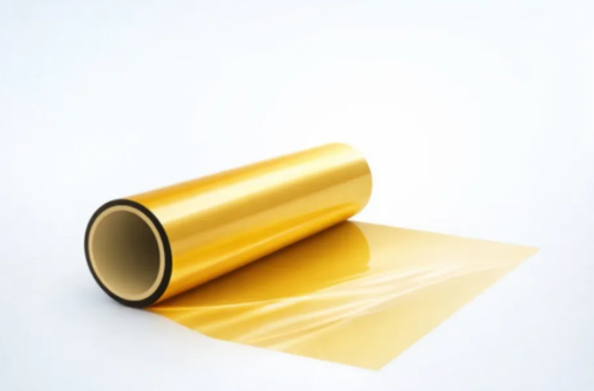
Asahi Kasei has developed a new type of photosensitive polyimide film that aligns with the semiconductor industry's trend toward panel-level packaging. This product combines the core technological advantages of the company's liquid photosensitive polyimide and dry film photoresist, effectively enhancing the production efficiency and yield of the new generation of packaging processes.
This film integrates the characteristics of two types of products: it retains the performance of Pimel liquid photosensitive polyimide materials used for buffer coatings and passivation layers, while also incorporating Sunfort dry film photoresist technology that can temporarily photolithographically pattern circuits on substrates and wafers. The product has now been handed over to customers for testing and evaluation, and is expected to be officially launched to the market soon.
Enhance production efficiency
This new type of film can be uniformly and easily applied to large-size square panels via a lamination process, significantly improving the production efficiency of semiconductor packaging. The product is compatible with multi-layer insulation structure designs and will be used in the future for redistribution layers in semiconductor packaging as well as insulation layers in packaging substrates.
When used in combination with the Sunfort TA series, which can produce fine lines as narrow as 1 micrometer, the film allows the manufacturer to simultaneously create fine circuit patterns and insulating resin layers through a lamination process alone. Asahi Kasei is also concurrently advancing a compatible solution pairing the film with the Sunfort CX series to meet the high aspect ratio copper pillar fabrication requirements for 3D semiconductor packaging.
Aligned with market development needs
Nobuko Ueda, Senior Executive Director of Asahi Kasei's Electronic Materials Division, stated that the company is fully prepared to respond to the changing application needs of its customers.
“As AI chip performance continues to advance, advanced semiconductor packaging urgently requires large-size, high-precision assembly process technologies,” said Nobuko Ueda. “With this new photosensitive polyimide film, we help customers improve production yield and processing efficiency, while also driving the continued evolution and upgrading of advanced semiconductor packaging technologies.”
Listed as a core strategic business
According to Asahi Kasei, its electronics business has been positioned as the top-priority growth segment in the company’s medium-term management plan for collaborative expansion. Electronic materials such as Pimel photosensitive polyimide and Sunfort dry film photoresist are widely used in advanced semiconductor packaging applications. As chip packaging density continues to increase and interposer sizes for AI data centers gradually expand, market demand for related materials is steadily rising.
As packaging evolves from wafer-level to panel-level and three-dimensional integration becomes increasingly advanced, circuit routing grows more intricate and the number of stacked layers continues to increase, which also places higher demands on the overall performance of packaging materials.
Asahi Kasei, founded in 1922, is a diversified multinational corporation with a global workforce of 50,000 employees. Its business spans three sectors—healthcare, homes and living, and materials—and it advances sustainability through a wide range of diversified solutions.
【Copyright and Disclaimer】This article is the property of PlastMatch. For business cooperation, media interviews, article reprints, or suggestions, please call the PlastMatch customer service hotline at +86-18030158354 or via email at service@zhuansushijie.com. The information and data provided by PlastMatch are for reference only and do not constitute direct advice for client decision-making. Any decisions made by clients based on such information and data, and all resulting direct or indirect losses and legal consequences, shall be borne by the clients themselves and are unrelated to PlastMatch. Unauthorized reprinting is strictly prohibited.
Most Popular
-

A Look at the Material Suppliers Behind SpaceX
-

Government's Triple Action, Enterprises' Three Arrows in Five Days, Semiconductor Reshuffle! What Signal Does Japan's Chemical Industry Release?
-

Fire breaks out at jiangsu meiside!
-

Name change without tax change: POM Anti-Dumping Duty Rate Inheritance Implemented
-

Ethylene: Production Capacity Accelerates Expansion, Global Industry Landscape Is Being Reshaped