



Japan Plans To Sell Lithography Giant JSR! Fujifilm And Mitsubishi Chemical Interested In Taking Over, How Much Time Window Is Left For China?
On May 28, 2026, a Reuters report sent shockwaves through the semiconductor materials industry: Japan’s government-backed Japan Investment Corporation (JIC) is considering selling chip materials maker JSR.
Two years ago, this government-backed fund privatized JSR at a price of $6 billion, with the original intention of leveraging this photoresist giant to promote the integration of Japan’s materials industry. Now, as the AI chip boom pushes up the valuations of companies in the semiconductor supply chain, JIC is already considering cashing out.
图源:JSR株式会社
Fujifilm and Mitsubishi Chemical have both expressed interest in an acquisition.On the day the news broke, Fujifilm’s shares closed up 3%, while Mitsubishi Chemical’s losses also narrowed significantly. The capital market told us in the most direct way possible just how hot the photoresist business is right now.
Who exactly is JSR? Why is photoresist worth so much? And where do Chinese manufacturers stand? Taken together, these questions happen to provide a clear way to explain the industry.
JSRA company that has been“national will” company
JSR was founded in 1957 and initially started as a synthetic rubber company, with the name JSR being an abbreviation for Japan Synthetic Rubber. Later, it transformed into a semiconductor materials company, dedicating several decades to the field of photoresists, ultimately becoming one of the most indispensable suppliers in the world.
For the fiscal year ended March 2026, JSR recorded revenue of ¥400.7 billion and net profit of ¥60.7 billion (about US$380 million), fully rebounding from the losses it had previously suffered due to its life sciences business. JIC originally acquired it as a key piece in its plan to drive a restructuring of Japan’s materials industry. Now, as the AI boom lifts valuations across the chip supply chain, JIC may have a chance to lock in a handsome exit gain.
For Fujifilm, acquiring JSR would mean firmly securing the top position in the global photoresist market; for Mitsubishi Chemical, it would mean extending from upstream chemical feedstocks all the way to core end materials, completing a textbook case of vertical integration across the value chain. Regardless of who ultimately wins the deal, JSR’s valuation logic has long ceased to be that of an ordinary materials company—it is more like a strategic bargaining chip.
Photoresist: the chip’s“ ”
To understand why a photoresist company is worth $6 billion, one must first understand what photoresist is.
The simplest analogy: photoresist is equivalent to the "film" in chip manufacturing. The core process of semiconductor manufacturing is photolithography—using light to "print" circuit patterns onto silicon wafers. Photoresist is the photosensitive material coated on the surface of the wafer; the areas exposed to light undergo a chemical reaction, and after development, form precise circuit patterns, which are then etched into the circuit through the etching process. This step directly determines the process precision and yield of the chips.
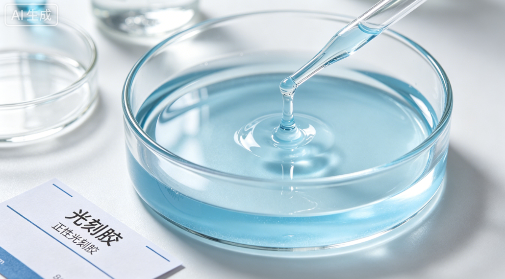
Photoresist (Image source: Doubao AI)
According to the wavelength of the exposure light source, photoresists are classified into several types in descending order of wavelength: G-line (436 nm), I-line (365 nm), KrF (248 nm), ArF (193 nm), and EUV (13.5 nm). The shorter the wavelength, the finer the lines that can be “written,” and the more advanced the process node it represents. KrF corresponds to mature process nodes above 28 nm, ArF corresponds to 14 nm to 28 nm, ArF immersion (ArFi) corresponds to 7 nm to 14 nm, and EUV is the standard for TSMC’s 2 nm and below processes.
At the core of each generation of photoresist lies an extremely complex chemical formulation—a precise combination of polymer resins, photoacid generators (PAGs), solvents, and various additives. Any flaw in any one of these elements can lead to lithography defects. Even more challenging, the validation cycle is extremely long: from testing to volume production, it often takes one to two years for a fab to qualify a material. Once certified, the cost of switching suppliers is very high. This is the industry’s natural moat: high technical barriers and strong customer stickiness.
Global Landscape: How Deep Is Japan’s Moat?
In the global photoresist market, Japanese companies collectively account for more than 80% of the market share. JSR, Tokyo Ohka Kogyo (TOK), and Shin-Etsu Chemical are known as the industry’s three major players.Fujifilm and Sumitomo Chemical each hold a place, while South Korea’s Dongjin is one of the few non-Japanese players able to enter this market, and the United States’ DuPont has a presence in the specialty photoresist segment.
The most difficult market to break into is EUV photoresists. EUV technology imposes extremely stringent requirements on the purity, uniformity, and photosensitivity of photoresists. JSR is the world’s leading supplier of EUV photoresists and is regarded as holding a monopolistic position. With the explosive growth in demand for Nvidia AI chips, TSMC’s CoWoS packaging, and the full-scale advancement of more advanced 2nm processes, demand for EUV photoresists is growing exponentially. This is also the core reason behind JSR’s surging valuation.
What is more concerning is that the photoresist industry has recently experienced another supply-chain shock: the US–Iran conflict has disrupted petrochemical logistics in the Strait of Hormuz.Key solvent raw materials for photoresists—propylene glycol monomethyl ether (PGME) and propylene glycol monomethyl ether acetate (PGMEA)—were once in tight supply, prompting Japanese giants to even consider sourcing alternative raw materials from China or South Korea.Short-term supply chain anxiety has instead accelerated downstream wafer fabs' willingness and urgency to adopt domestic solutions, indirectly opening a door for Chinese photoresist companies.
One hand has broken through, one hand...
The landscape of domestic Chinese photoresist companies is much like a marathon course with runners at different stages of progress: those at the front are already in mass production, those in the middle are undergoing qualification and certification, and those at the back are still in the R&D stage.
For display photoresists, the progress in this field shows that the localization rate is already quite high. Fuyang Xinyi HuacaiIt is a typical representative in this niche segment — on November 28, 2025, Xinyihua Materials’ Lu’an production base was officially put into operation, with planned annual output of 10,000 tons of display photoresists and 2,000 tons of semiconductor photoresists. Its display photoresist shipments had already ranked first in China, supplying major panel manufacturers such as BOE and TCL China Star. On April 22, 2026, the company updated its STAR Market IPO tutoring filing once again, changing its tutoring institutions to CICC and Kaiyuan Securities, indicating a significant acceleration in its capital market process.
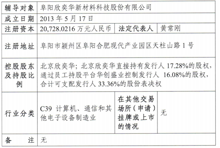
Image source: Fuyang Xinyihua Materials
Photoresist used in semiconductor wafer front-end processes is the real hard battle.This type of photoresist is cleaned off after each lithography step, making it a high-frequency consumable with large demand and extremely high technical requirements, and its core patents are almost entirely controlled by companies in Japan and the United States.
KrFRegarding ArF photoresists,March 19, 2025 marked a milestone: the “300-ton annual KrF/ArF photoresist industrialization project” of a controlled subsidiary of Super Chemicals Co., Ltd. officially went into production. This is the first domestic high-end wafer photoresist production line covering the entire process from “organic synthesis—polymer synthesis—purification—photoresist blending,” truly achieving full-chain self-reliance and controllability from key raw materials to finished photoresist products.
April 17, 2026Weimai New MaterialsA production base for the core materials of high-end DUV photoresists—the largest of its kind in China—has been put into operation in Hefei, covering photoacid generators, resins, and photoinitiators, with a planned annual capacity of 100 tons. Technological breakthroughs have already been achieved for the 7/14 nm process nodes.
Photosensitive polyimide (PSPI) for advanced packagingThe competition is equally intense. On April 21, 2026,Aisen Co., Ltd.It announced that its self-developed low-temperature PSPI product had secured an order from a well-known industry customer, breaking the decades-long technological monopoly of foreign companies in low-temperature PSPI materials. On April 24, the company also announced plans to raise RMB 524 million to build Phase I of its East China manufacturing base for integrated circuit materials, which will have an annual production capacity of 2,000 tons of photoresist and 500 tons of supporting photoresist resin.
April 24,Ruilian New MaterialsRedirect RMB 75 million of the raised funds to the PSPI material industrialization project.Strong New Materials Eight Hundred Million Spacetimeare also in the customer validation and pilot production stages, respectively.
AILarge models enter photoresist research.
On May 12, 2026, a rather notable event took place. The official WeChat account of the Shanghai Artificial Intelligence Laboratory announced that, under the National New Generation AI Major Project, the Shanghai AI Laboratory, in collaboration with Xiamen University and the Suzhou National Laboratory, had built a closed-loop R&D system of “AI-driven decision-making + automated synthesis” based on the InternLM scientific foundation model, and successfully developed high-purity, highly consistent KrF photoresist resin.
The significance of this achievement goes beyond yet another technological breakthrough. The development of photoresist resins has long relied on an “experience-driven” trial-and-error approach, requiring researchers to screen, one by one, thousands of monomer ratios, polymerization systems, and reaction conditions. Development cycles are measured in months and are highly susceptible to human operational errors. High-end resins are most vulnerable to two issues: trace metal impurities, which affect photosensitive performance, and uneven molecular weight distribution, which leads to performance drift between batches. These two challenges, however, are precisely the most difficult for traditional processes to control consistently.
Shanghai AI Laboratory’s approach is to build an intelligent system featuring a “decision–connectivity–execution–iteration” loop: AI models generate synthetic plans, and the Scientific Context Protocol (SCP) converts instructions into executable commands for automated platforms. After the physical laboratory completes high-throughput synthesis and characterization, data such as molecular weight and thermal stability are automatically fed back to the AI, driving the algorithm to optimize the next round of plans. This closed-loop system has enabled the PDI (polydispersity index) of photoresist resins to be stably controlled below 1.3, metal impurity content to be controlled below 10 ppb, and batch-to-batch stability to reach ±10%. On the industry side, Xiamen Hengkang New Materials has completed resin adaptation, with key performance indicators meeting expectations, and is about to enter client validation.
The value of this route lies in the fact that it makes the stable production of high-end photoresist resins no longer dependent on the “black-box expertise” accumulated over decades by a very small number of overseas suppliers, but instead opens up a standardized, rapidly iteratable engineering pathway.
Written at the end
In the past two years, China’s photoresist industry has seen frequent activity, but we must also soberly recognize where the gaps remain.
In terms of production capacity, Dinglong Co., Ltd. is currently the only domestic company to have established a kiloton-scale mass production line for wafer photoresists, while most other enterprises have mass production capacities of less than 500 tons and are mainly concentrated in mid- to low-end products. In terms of supply chain stability, the localization rate of key monomers for PSPI is only about 60%, and the risk of fluctuations in upstream raw materials remains. On the technical front, domestic high-end photoresists for processes below 7nm are still in the R&D stage, and the core patent barriers for EUV photoresists are almost impossible to circumvent. According to Frost & Sullivan data, the domestic semiconductor photoresist market is expected to reach RMB 15.03 billion by 2028—an opportunity, but also a gap yet to be filled.
Another structural variable worth watching is capital enthusiasm. The IPOs or refinancing efforts currently being pursued by companies such as Xinyihua Materials and Eson shares reflect the capital market’s high expectations for this sector. Against the backdrop of three overlapping drivers—supply chain security concerns, explosive demand for AI chips, and capacity expansion at domestic wafer fabs—the capitalization and industrialization of China’s domestic photoresist industry are indeed accelerating.
Returning to the question of JSR’s ownership change itself: whether Fujifilm or Mitsubishi Chemical ultimately takes over, the landscape of Japan’s photoresist industry will not be fundamentally overturned; in fact, it may become even stronger through further consolidation. For Chinese companies, the real window of opportunity may lie not in the capital maneuvering of any single giant, but in the substitute space exposed by every supply-chain crisis and the customer validation opportunities brought by every technological breakthrough.
Editor: Lily
Sources: Reuters, Electronic Engineering Times, DT New Materials, etc.
【Copyright and Disclaimer】This article is the property of PlastMatch. For business cooperation, media interviews, article reprints, or suggestions, please call the PlastMatch customer service hotline at +86-18030158354 or via email at service@zhuansushijie.com. The information and data provided by PlastMatch are for reference only and do not constitute direct advice for client decision-making. Any decisions made by clients based on such information and data, and all resulting direct or indirect losses and legal consequences, shall be borne by the clients themselves and are unrelated to PlastMatch. Unauthorized reprinting is strictly prohibited.
Most Popular
-

A Look at the Material Suppliers Behind SpaceX
-
BASF, Selling Again!
-
BASF Cuts Core Business As It Exits All Non-Core Operations, Triggering A New Round Of Industry Restructuring
-
Eastman France PET Depolymerization Plant: Project "Alive," But Construction Paused
-
Mitsubishi Chemical Plans To Split Petrochemical Business By 2028